- Home (current)
- SoC
- Cloud Service
- News
- Contact
- English
17/06
ThursdayShenju Technology's world's first BLE application solution using long distance wireless power supply
Shenju Technology's world's first BLEapplication solution using wireless power supply in June 2021,Shenju Technology successfully designed a prototype based on the Atmosic M3 SOC series energy harvesting technology. This application uses the radio frequency carrier signal in the environment to realize long-distance wireless power supply, so that BLE equipment can self sustain without a battery.
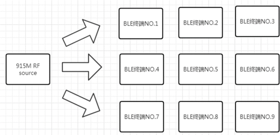
Based on battery-free application scenarios, Shenju Technology uses a 915 MHz radio frequency IC, which combines a power amplifier chip and filter as a radio frequency source to provide remote power supply to multiple BLE equipment at the same time.
On the receiving end, Shenju Technology uses the world's lowest power consumption BLE 5.0 SOC-Atmosic M3 series ATM3202 chip as the BLE terminal and harvesting radio frequency energy.
The radio frequency source and BLE terminal equipment are as follows:
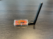
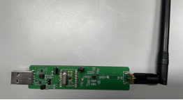
(BLE Equipment) (915MHZ RF signal source)
Place 9 BLE equipment in a 50cm*50cm*60cm display rack. The radio frequency source is powered by a portable power bank. Observe the red LED of the BLE terminal at a close distance. You can observe that these 9 LED lights flash once every second. At the same time, through the mobile phone APP (such as lightblue/nrfconnect) Search BLE equipment broadcast data, you can get the corresponding device name (xx_ShenJu) correctly.
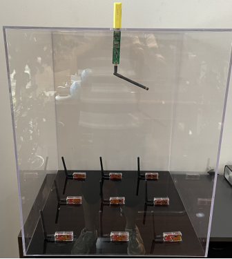
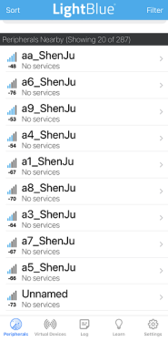
(Complete display cabinet) (Mobile Apps)
Atmosic M3 series energy harvesting principlePMU power management has two acquisition input pins-HARV1 IN pin and HARV OUT pin, among them HARV1 IN pin is used to connect the antenna, battery VBAT and capacitor VSTORE are independent energy storage components, so that the PMU in the chip can extract electric energy from it.
In the current solution, the BLE chip relies on the antenna to collect energy to maintain operation, and stores the excess energy in the energy storage capacitor at VSTORE end. During the period of insufficient energy harvesting, the PMU will use the power on the VSTORE until the VSTORE voltage value is the threshold for low Bluetooth operation.
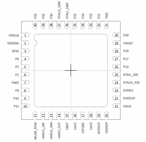
(ATM3202 Pin Assignment )
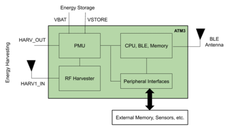
(BLE Circuit Block Diagram)
After the radio frequency source sends out the radio frequency signal, the circuit of the BLE SOC ATM3202 chip pins HARV1 INP and HARV1 INN collects energy through the antenna, the energy storage capacitor voltage rises, and the ATM3202 chip in the ultra-low-power standby state is awakened to start working. During the application demonstration of this solution, the BLE equipment will start the broadcast and the LED will start flashing. At the same time, the user can obtain the broadcast data through the mobile phone APP.
The question that users are most concerned about should be, maximum distance between RF power source with the BLE equipment.
Take the radio frequency source transmitting power of 36 dBm. For example, the 915 MHz signal source can maintain the BLE equipment to function at a distance of 5 meters. The relationship between the power supply distance of the radio frequency source and the power consumption is shown in the figure:
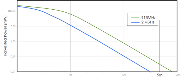
( X-axis: RF energy collection distance Y-axis: RF energy collection power)
For more information about the features of Atmosic's M2 and M3 series, please stay tuned.
Related News
- Industry NewsAtmosic World Lowest Power Consumption Battery-Free BLE M3 SoC Named a CES 2020 Best of Innovation Honoree
- Industry NewsAtmosic World Lowest Power Consumption BLE 5.0 SoC with Energy-Harvesting Features That Target ‘Forever Power’ for IoT Devices
- Product IntroductionUsing Atmosic Lowest Power Consumption BLE SoC Can Help Beacon to Last Forever Battery Free
